
Report an Error


NVIDIA RTX A2000 Max-Q 8 GB
- Graphics Processor
- GA107
- Cores
- 2560
- TMUs
- 80
- ROPs
- 48
- Memory Size
- 8 GB
- Memory Type
- GDDR6
- Bus Width
- 128 bit
GPU
Recommended Gaming Resolutions:
- 1920x1080
- 2560x1440
- 3840x2160
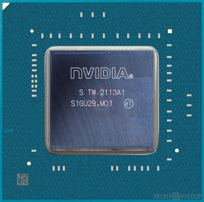
The RTX A2000 Max-Q 8 GB is a professional mobile graphics chip by NVIDIA, launched on April 12th, 2021. Built on the 8 nm process, and based on the GA107 graphics processor, the chip supports DirectX 12 Ultimate. The GA107 graphics processor is an average sized chip with a die area of 200 mm² and 8,700 million transistors. It features 2560 shading units, 80 texture mapping units, and 48 ROPs. Also included are 80 tensor cores which help improve the speed of machine learning applications. The card also has 20 raytracing acceleration cores. NVIDIA has paired 8 GB GDDR6 memory with the RTX A2000 Max-Q 8 GB, which are connected using a 128-bit memory interface. The GPU is operating at a frequency of 607 MHz, which can be boosted up to 1177 MHz, memory is running at 1375 MHz (11 Gbps effective).
Its power draw is rated at 95 W maximum. This device has no display connectivity, as it is not designed to have monitors connected to it. Rather it is intended for use in laptop/notebooks and will use the output of the host mobile device. RTX A2000 Max-Q 8 GB is connected to the rest of the system using a PCI-Express 4.0 x16 interface.
Its power draw is rated at 95 W maximum. This device has no display connectivity, as it is not designed to have monitors connected to it. Rather it is intended for use in laptop/notebooks and will use the output of the host mobile device. RTX A2000 Max-Q 8 GB is connected to the rest of the system using a PCI-Express 4.0 x16 interface.
Graphics Processor
Mobile Graphics
- Release Date
- Apr 12th, 2021
- Generation
-
Ampere-MW
(Ax000)
- Predecessor
- Quadro Turing-M
- Successor
- Ada-MW
- Production
- Active
- Bus Interface
- PCIe 4.0 x16
Relative Performance
Based on TPU review data: "Performance Summary" at 1920x1080, 4K for 2080 Ti and faster.
Performance estimated based on architecture, shader count and clocks.
Clock Speeds
- Base Clock
- 607 MHz
- Boost Clock
- 1177 MHz
- Memory Clock
-
1375 MHz
11 Gbps effective
Memory
- Memory Size
- 8 GB
- Memory Type
- GDDR6
- Memory Bus
- 128 bit
- Bandwidth
- 176.0 GB/s
Render Config
- Shading Units
- 2560
- TMUs
- 80
- ROPs
- 48
- SM Count
- 20
- Tensor Cores
- 80
- RT Cores
- 20
- L1 Cache
- 128 KB (per SM)
- L2 Cache
- 2 MB
Theoretical Performance
- Pixel Rate
- 56.50 GPixel/s
- Texture Rate
- 94.16 GTexel/s
- FP16 (half)
- 6.026 TFLOPS (1:1)
- FP32 (float)
- 6.026 TFLOPS
- FP64 (double)
- 94.16 GFLOPS (1:64)
Board Design
- Slot Width
- IGP
- TDP
- 95 W
- Outputs
- Portable Device Dependent
- Power Connectors
- None
- Board Number
- E4736 SKU 10
Graphics Features
- DirectX
- 12 Ultimate (12_2)
- OpenGL
- 4.6
- OpenCL
- 3.0
- Vulkan
- 1.3
- CUDA
- 8.6
- Shader Model
- 6.8
GA107 GPU Notes
| Ray Tracing Cores: 2nd Gen Tensor Cores: 3rd Gen NVENC: 7th Gen NVDEC: 5th Gen PureVideo HD: VP11 VDPAU: Feature Set K Latest Drivers: Windows 7 / 8 / 8.1 (x64): GeForce Release 474.89 Windows 10 / 11 (x64): GeForce Release: Latest Quadro Release: Latest Data Center Release: Latest |
Devices based on this design (3)
| Name | GPU Clock | Boost Clock | Memory Clock | Other Changes |
|---|---|---|---|---|
| 607 MHz | 1177 MHz | 1375 MHz | ||
| 990 MHz | 1462 MHz | 1375 MHz | ||
| 862 MHz | 1335 MHz | 1368 MHz |
Apr 7th, 2025 10:28 HKT
change timezone
Latest GPU Drivers

New Forum Posts
- 9070XT or 7900XT (42)
- No idea how many watts this USB-C port will supply? (3)
- gpu heirarchy/performance/benchmarks- whos lying? (39)
- Share your AIDA 64 cache and memory benchmark here (3049)
- I dont think the HT-Omega sound card company has anyone running it anymore. Cant get responses from customer service for last 2 years. (2)
- A dozen drivers for HD4670, and which do I choose? (10)
- What's your latest tech purchase? (23486)
- What are you playing? (23349)
- i7-13700HX capped at 25 watts (13)
- Weird games on rtx 3070ti (1)

Popular Reviews
- ASUS Prime X870-P Wi-Fi Review
- UPERFECT UStation Delta Max Review - Two Screens In One
- PowerColor Radeon RX 9070 Hellhound Review
- Upcoming Hardware Launches 2025 (Updated Apr 2025)
- Corsair RM750x Shift 750 W Review
- Sapphire Radeon RX 9070 XT Pulse Review
- Sapphire Radeon RX 9070 XT Nitro+ Review - Beating NVIDIA
- DDR5 CUDIMM Explained & Benched - The New Memory Standard
- AMD Ryzen 7 9800X3D Review - The Best Gaming Processor
- AMD Ryzen 9 9950X3D Review - Great for Gaming and Productivity
Controversial News Posts
- MSI Doesn't Plan Radeon RX 9000 Series GPUs, Skips AMD RDNA 4 Generation Entirely (146)
- NVIDIA GeForce RTX 5060 Ti 16 GB SKU Likely Launching at $499, According to Supply Chain Leak (135)
- Microsoft Introduces Copilot for Gaming (124)
- AMD Radeon RX 9070 XT Reportedly Outperforms RTX 5080 Through Undervolting (119)
- NVIDIA Reportedly Prepares GeForce RTX 5060 and RTX 5060 Ti Unveil Tomorrow (115)
- Over 200,000 Sold Radeon RX 9070 and RX 9070 XT GPUs? AMD Says No Number was Given (100)
- NVIDIA GeForce RTX 5050, RTX 5060, and RTX 5060 Ti Specifications Leak (97)
- Nintendo Switch 2 Launches June 5 at $449.99 with New Hardware and Games (92)